Amorphization and Ablation of Crystalline Silicon Using Ultrafast Lasers: Dependencies on the Pulse Duration and Irradiation Wavelength
-
Study reveals how ultrashort laser pulses can transform crystalline silicon into amorphous silicon, optimizing key processes in advanced semiconductor device manufacturing and silicon photonics.
Madrid / August 29, 2024
Researchers from the Laser Processing group at the CSIC Institute of Optics and the LP3 Laboratory belonging to the Aix Marseille University and the CNRS have published a new study in the journal Laser and Photonics Reviews in which the conditions for transforming crystalline silicon into amorphous silicon by irradiation with ultrashort laser pulses (less than a picosecond) are characterized. To this end, the fluence limits for achieving this transformation have been studied, including an extensive bibliographic review, and the maximum depths of this transformation are characterized using different pulse durations, different wavelengths, and samples with different crystallographic orientations.
Latest news
Silicon photonics is a key field in the development of advanced technologies for the manufacture of electronic and photonic devices, taking advantage of the properties of silicon, a material that is omnipresent in today’s semiconductor industry.
One of the most important processes in this field is the controlled modification of the structure of silicon using laser techniques. These techniques allow the properties of the material to be altered so that it can be used in different applications, from chip manufacturing to the development of optical devices.

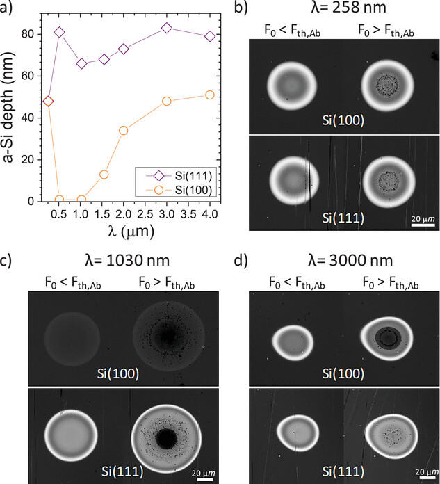
a) Thickness of the amorphous layer as a function of laser wavelength for single-pulse irradiations. Samples: Si(111) (type n. 0.002–0.005 Ω cm) and Si(100) (intrinsic. 200–600 Ω cm). b–d) Optical microscopy images of laser-induced modifications at different irradiation wavelengths on Si(111) and Si(100) (both intrinsic) with illumination at λLED = 460 nm. Points correspond to modifications at peak fluences close to (below and above) the threshold for ablation (b) F0 = 200 and 260 mJ cm−2; c) F0 = 330 and 480 J cm−2; d) F0 = 490 and 720 J cm−2). / Laser and Photonics Reviews
The published study focuses on understanding how the duration of the laser pulse and the irradiation wavelength influence the amorphization and ablation processes of the crystalline silicon surface.
The melting of a part of the surface by laser and subsequent annealing is an already established technique to allow the recrystallization of the silicon surface in an amorphous form. The amorphization process of silicon surfaces has as its main application the creation of surface waveguides (like the optical fiber in our homes but on a chip). This is achieved by the higher refractive index of the amorphous phase compared to the crystalline phase, which causes the light to bounce around inside the waveguide and not be able to escape. The challenge today is to achieve a sufficient thickness of the amorphous layer to satisfy the waveguide conditions in telecommunications.
In order to carry out the study, the current literature on these topics has been compared with the experimental data and conclusions of the research group, and in this work many of these new data related to the role of the laser wavelength for the processing of Silicon have been published.
The validity of the assumed relationship between the amorphization and melting thresholds has also been experimentally demonstrated by means of time-resolved microscopy measurements.
This work is part of the scientific efforts in the development of models that can predict the response of silicon to different femtosecond laser processes and thus further develop the so-called “silicon photonics”.
Article: Mario Garcia-Lechuga, Noemi Casquero, Jan Siegel, Javier Solis, Raphael Clady, Andong Wang, Olivier Utéza, and David Grojo. “Amorphization and Ablation of Crystalline Silicon Using Ultrafast Lasers: Dependencies on the Pulse Duration and Irradiation Wavelength.” Laser and Photonics Reviews 2024, 2301327
IO-CSIC Communication cultura.io@io.cfmac.csic.es
Related news
The Institute of Optics joins the celebration of 11F
Full and equal access and participation of women and girls in science and technology Madrid / January 31, 2025In recent decades, the international...
Optoplasmonic tuneable response by femtosecond laser irradiation of glass with deep-implanted gold nanoparticles
Ion implantation of Au2+ at MeV energies has enabled the creation of nanoparticles embedded at greater depth, resulting in a Fabry-Perot cavity...
On November 20th, David Grojo from CNRS will give a lecture entitled “New Dimensions Open to Ultrafast Laser Material Modifications”
Madrid / November 13, 2024On Wednesday, November 20th at 11:30 a.m. we will have a seminar organized by the Laser Processing Group in the conference...


