Low-Loss Directional Coupler for the C, L and U Bands Based on Subwavelength Gratings
-
New advance in technology Directional couplers enable efficient and customizable power distribution in photonic circuits.
Madrid / November 28, 2023
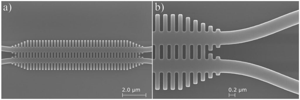
Researchers from the spin-off Alcyon Photonics, the Optics Institute of the CSIC and the CNRS of Paris-Saclay University have published an improvement in the technology of directional couplers, essential components for the efficient division and distribution of energy in integrated photonic circuits. The team has developed a low-loss directional coupler that covers most of the bands used in telecommunications, and is based on the innovative use of subwavelength gratings. This novel design allows for an adaptable power distribution ratio over a wide bandwidth, making it a versatile and efficient tool for multiple applications in the field of photonics.
Latest news

Directional couplers play a critical role in optical power distribution in photonic integrated circuits, especially in applications such as wavelength division multiplexing (WDM) and optical filtering. Despite the progress made so far, the search continues for architectures that offer customizable coupling ratios at increasingly wider bandwidths, while maintaining compact size and low losses.
In this study, published in IEEE Photonics Technology Letters, the team has presented a compact and highly efficient directional coupler, based on the phenomenon of scattering through subwavelength metamaterials. By using wavelength gratings, the researchers have managed to experimentally demonstrate that their device has low losses and a flat spectral response over a wide bandwidth that completely encompasses the C, L and U telecommunications bands, which span from 1505 nm to 1675 nm.
Experimental measurements revealed average losses below 0.24 dB and coupling ratio deviations below ±1 dB over a bandwidth of 170 nm. These values meet the stringent performance requirements of power dividers used in multiple coupling stages in photonic circuits. Additionally, the maximum coupling ratio deviations within the individual C, L, and U bands were reduced to ±0.3 dB, ±0.5 dB, and ±0.5 dB, respectively.
PhD student Jaime Vilas commented: “Our low-loss directional coupler represents a significant step in improving the efficiency and customization of power distribution in photonic integrated circuits. The ability to tailor the coupling ratio in a Wide bandwidth, coupled with low losses and flat spectral response, makes it perfect for applications such as optical filtering and wavelength division multiplexing. The coupler’s compact design and exceptional performance make it a promising tool for the implementation of multistage optical filters”.
This advance in directional coupler technology not only has an impact on the field of photonics, but can also contribute to the reduction of manufacturing costs in the integrated circuit industry, thanks to the use of platforms SILICON-ON-INSULATOR (SOI) and to the maturity of microelectronics manufacturing.
The research team continues to work on optimizing the design of the directional coupler, with the aim of further improving its performance at higher wavelengths. This technology is expected to drive the development of more efficient and advanced photonic systems, with applications in areas such as optical communications, quantum computing and on-chip spectrometers.
IO-CSIC Communication
cultura.io@io.cfmac.csic.es
Related news
Tunable bound states in the continuum in active metasurfaces of graphene disk dimers
Madrid / December 12, 2023A research team made up of researchers from the Institute of Structure of Matter and the Optics Institute of the CSIC, the...
Next scientific coffee by Pedro Corredera on July 20
Madrid / July 12, 2023This is the third talk of the course. On May 20, 2019, the new definitions of the SI units of measurement based on universal...
A 25 km pulsed laser to help the environment
Madrid / June 21, 2023A team from the CSIC Institute of Optics, in collaboration with the University of Tampere, in Finland, has just taken a new...


