Experimental characterization of an ultra-broadband dual-mode symmetric Y–junction based on metamaterial waveguides

-
The device has losses of as only 0.3 dB for the fundamental transmission mode in a 260 nm bandwidth.
-
For secondary mode the losses are below 1 dB in a 100 nm bandwidth.
Madrid / November 30, 2022
Measurements made using successive dividers have shown power losses below 0.3 dB when the fabrication resolution is 50 nm. For lower fabrication resolutions (100 nm), the losses are kept below 0.5.
Recently, this same group proposed this architecture for manufacturing error-tolerant Y-joints. However, this earlier study only covered simulation results and preliminary measurements, awaiting this expanded experimental study.
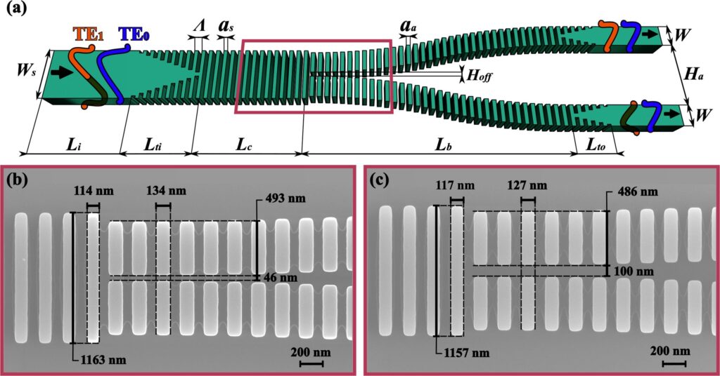
This “Y” power divider is based on subwavelength lattice metamaterials for integration into silicon photonic circuits.
Latest news

Scheme of the “Y” power divider and microscopic view of the metamaterial for two manufacturing processes with different resolution.
Metamaterials of subwavelength networks
Oversimplifying, subwavelength lattices are made up of pieces lined up like a path of dominoes, where these pieces are much smaller than the wavelength of the light that travels through them. It happens that in this way the light propagates along the path as if it were a new homogeneous material (what is known as a metamaterial), with the advantage that its optical properties can be modified at will.
This innovative solution has already been successfully applied to many other technologies.
Silicon Photonics
Silicon photonic integrated circuits are beginning to be treated as compact and efficient solutions designed to overcome the limitations of classical circuits based on copper wires.
Optical power dividers are a fundamental component in integrated photonic circuits. They are used to distribute light across the chips and are also key elements in building more complex devices. A power splitter has yet to be found that meets all the desirable requirements: manufacturing error tolerance, low power loss, small footprint, and works well with various optical modes.
Today there are many lines of research working with different power divider architectures. However, the resolution of current manufacturing processes result in minimum manufacturable sizes, limiting the design of this type of device. Specifically, in “Y” power dividers, it results in imperfections at the tip of the joint between its two arms, which generates significant power losses. Thanks to the use of metamaterials in these devices, it is possible to deconfine the fundamental mode in the vicinity of the junction and thus successfully mitigate losses.
Applications
These new power dividers, being a basic component in photonic circuits, open up promising prospects for expanding the scope of photonic integration to many fields of modern technology such as 5G mobile communications, Internet of Things, quantum photonics, and solutions on a chip for laboratory applications.
Related news
Aitor Villafranca, Spanish National Research Award 2024
He has received the award in the Angela Ruiz Robles Category, in Knowledge Transfer These awards are the most important recognition in Spain...
Normal Incidence Excitation of Out-of-Plane Lattice Resonances in Bipartite Arrays of Metallic Nanostructures
Madrid / January 15, 2024A team of researchers from the Institute of Optics of the CSIC and the Italian Institute of Technology have achieved a new...
Tunable bound states in the continuum in active metasurfaces of graphene disk dimers
Madrid / December 12, 2023A research team made up of researchers from the Institute of Structure of Matter and the Optics Institute of the CSIC, the...


