Versatile femtosecond laser interference patterning applied to high-precision nanostructuring of silicon
-
A novel femtosecond laser technique improves silicon nanostructuring capabilities with a commercial laser.
-
The achieved laser interference patterns enable the fabrication of periodic surface structures with sizes up to 120 nm.
Madrid / August 9, 2024
A team of researchers from the Laser Processing Group at IO-CSIC has published a scientific article in the journal Optics & Laser Technology in which they present an innovative nanostructuring technique based on the interference of a commercial amplified femtosecond laser. The scientists were able to improve on previous work by manufacturing gratings with tunable periods of up to 650 nm and amorphous silicon dots with feature sizes of up to 120 nm. This versatile technique has the potential for direct application in industrial processes for manufacturing high-precision materials.
Latest news
In recent decades, nanostructuring of materials using ultrafast lasers has emerged as a promising field of research. These lasers heat the treated material less and achieve smaller and sharper resolution sizes compared to nanosecond lasers.
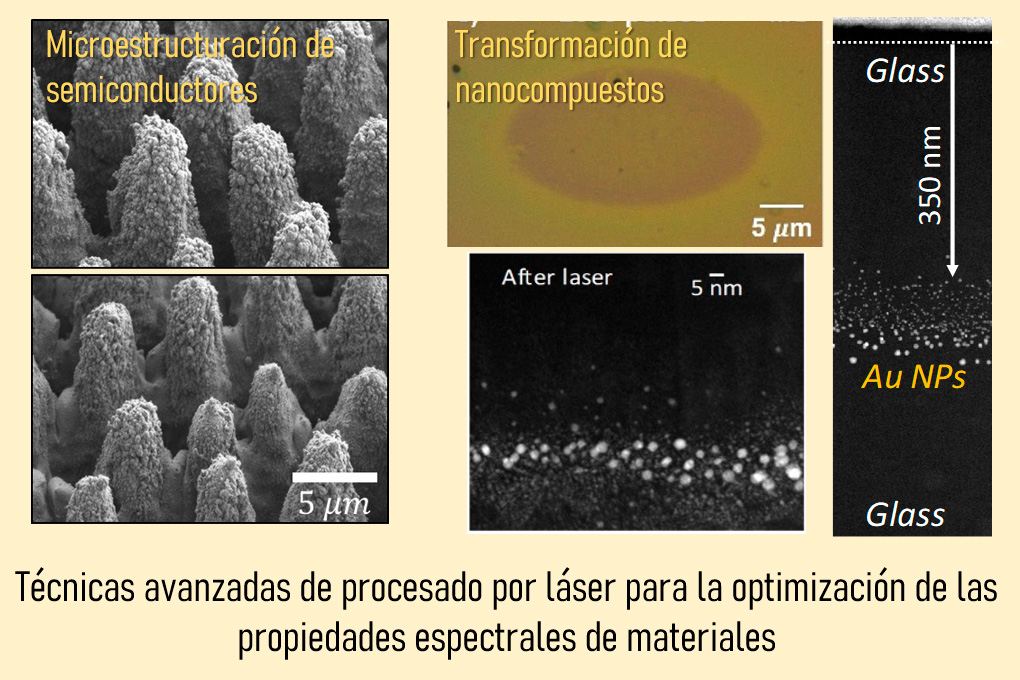
In this work, the research team has carried out an innovative study on silicon nanostructuring using interference from a commercial femtosecond amplified laser. The technique employed is based on direct laser interference patterning (DLIP), which enables the fabrication of high-precision periodic surface structures in a single pass. This approach exhibits exceptional versatility and significant potential for rapid and precise fabrication of metasurfaces in a wide range of materials, opening up new opportunities in nanoscale manufacturing and promising substantial impact in diverse fields such as photonics, biology, medicine, microfluidics and others.

The acronyms of the components of the setup are: aperture (A), half-wave plate (λ/2), quarter-wave plate (λ/4), polarizing beam splitter (PBS), focusing lens (FL), microscope objective (MO), tube lens (TL).
What is direct laser interference pattern?
The direct laser interference pattern (DLIP) technique is a technique that allows the fabrication of periodic nanoscale structures in a wide variety of materials and in large areas. This technique achieves that the laser with which the material is irradiated is periodically modulated by secondary beams so that instead of at a point the laser attacks the material forming a pattern in a single pass.
Related news

Amorphization and Ablation of Crystalline Silicon Using Ultrafast Lasers: Dependencies on the Pulse Duration and Irradiation Wavelength
Madrid / August 29, 2024Researchers from the Laser Processing group at the CSIC Institute of Optics and the LP3 Laboratory belonging to the Aix...
Predoctoral contract offer in the Laser Processing Group (4-year FPI contract)
Madrid / October 7, 2024The Laser Processing group of the Institute of Optics has published a vacancy to carry out a doctoral thesis entitled...

Dynamic restructuring of nickel sulfides for electrocatalytic hydrogen evolution reaction
Madrid / August 2, 2024An international team with the participation of the Laser Processing group of the CSIC Institute of Optics has published in...