Preferential out-of-plane growth of two-dimensional molybdenum diselenide flakes on laser-induced periodic surface structures
Madrid / July 29, 2024
Latest news

In the last decade, research into two-dimensional (2D) materials has aroused great interest due to their unique properties and broad potential in various areas, such as electronics, photonics, mechanics, and catalysis. In this context, transition metal dichalcogenides (TMDs) have emerged as an important class of 2D materials. Among them, molybdenum diselenide (MoSe2) has attracted attention due to its high electrical conductivity, superior to other well-studied TMDs. In addition, vertically oriented MoSe2 flakes offer promising characteristics for different applications, thanks to their aspect ratio (thicknesses of a few nanometers and sizes in the micrometer range) that provide them with a large active surface, which are crucial for catalytic reactions and applications in energy systems, chemical synthesis and environmental treatment.
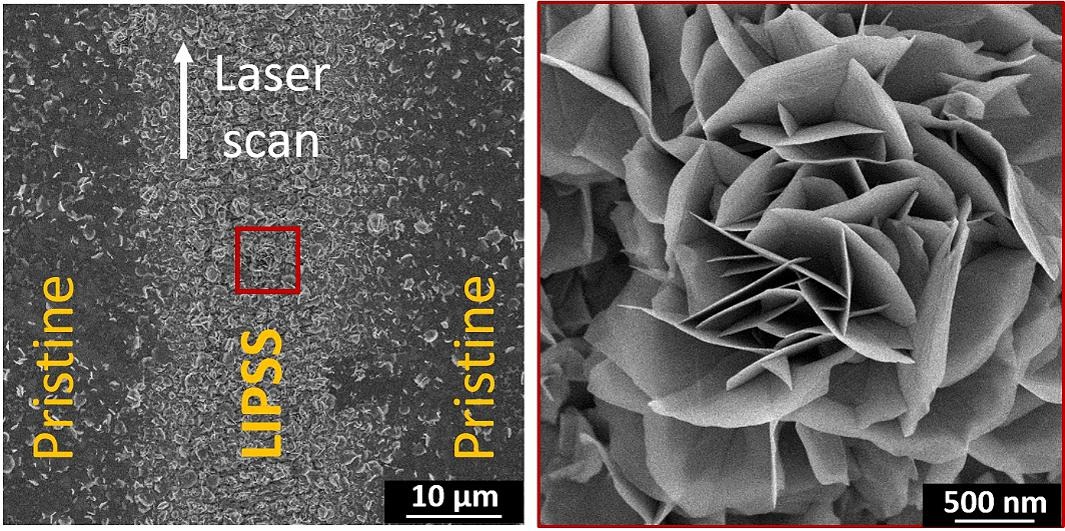
In this context, the team behind this work has explored a new strategy that allows the preferential out-of-plane growth of 2D MoSe2 flakes, combining thin film deposition methods on previously laser-structured substrates.
“The first step of our strategy consists of inducing a smooth topography on the surfaces of substrates of interest, both in dielectric and conductive materials, using ultrashort laser pulses. Subsequently, using the closed-space isothermal vapor deposition (ICSVD) technique, we synthesize MoSe2 on these substrates” explains Mario García Lechuga from the CSIC Institute of Optics and principal investigator of the project.
“Using scanning electron microscopy and Raman spectroscopy, we have characterized that in the modified substrate regions there is both a greater deposit of material and a preferential vertical orientation of the 2D MoSe2 flakes” adds Alejandro Fernández García from the Autonomous University of Madrid and first author of the article.
The authors are convinced that this technique can potentially be applied to any other two-dimensional Van der Waals material, which can be crucial for technological issues such as catalysis and electronic devices.
What is Raman scattering?
Raman scattering is the inelastic scattering of light that occurs when matter is irradiated by a monochromatic light source. After this monochromatic light has interacted with the sample, a very small part of the light has changed its wavelength.
Surface-enhanced Raman scattering (SERS) is a method used to amplify weak Raman signals. Raman signals are inherently weak due to the statistically low number of wavelength-shifted photons available for detection.
In SERS, nanostructured or roughened metal surfaces, typically gold or silver, are employed. Laser excitation of these metal structures drives surface charges to create a localized plasmon field, an enhanced electric field.
When a molecule is close to the surface and, consequently, to that enhanced electric field, a large enhancement in its Raman signal occurs, resulting in Raman signals several orders of magnitude larger than normal Raman scattering. In this way, it is possible to detect lower concentrations of the sought particles.
Article: A. Fernández García, R. Ariza, J. Solis, F. Agulló-Rueda, M. Manso Silvan, M. Garcia-Lechuga. “Out-of-plane preferential growth of 2D molybdenum diselenide nanosheets on laser-induced periodic surface structures”. Applied Surface Science, October 2024.
Related news
The Institute of Optics joins the celebration of 11F
Full and equal access and participation of women and girls in science and technology Madrid / January 31, 2025In recent decades, the international...
Optoplasmonic tuneable response by femtosecond laser irradiation of glass with deep-implanted gold nanoparticles
Ion implantation of Au2+ at MeV energies has enabled the creation of nanoparticles embedded at greater depth, resulting in a Fabry-Perot cavity...
On November 20th, David Grojo from CNRS will give a lecture entitled “New Dimensions Open to Ultrafast Laser Material Modifications”
Madrid / November 13, 2024On Wednesday, November 20th at 11:30 a.m. we will have a seminar organized by the Laser Processing Group in the conference...


