Optoelectronic properties of GaP:Ti photovoltaic devices
- UCM scientists, in collaboration with the IO-CSIC and the UAM, have developed a new solar cell based on GaP:Ti that increases light absorption at low energy.
- This breakthrough, published in the journal “Materials Today Sustainability”, opens the door to the manufacture of more efficient and sustainable solar cells.
Madrid / November 7, 2024
Latest news

Natural Slab Photonic Crystals as Biogenic, Customizable Nanomaterial for Label-Free Detection
Scientists demonstrate the potential of diatoms as photonic nanomaterials for sensing. The biogenic material is extracted directly from the microalgae and does not require markers, simplifying and reducing the cost of the sensor manufacturing process. Madrid / April...
The need for clean and renewable energy sources has multiplied research in the field of photovoltaics. Within this field, one of the most promising approaches to increase the efficiency of solar cells is the concept of intermediate band (IB) solar cells. This concept proposes the creation of a band of allowed states between the valence and conduction bands of a semiconductor, which would allow the absorption of photons with energies below those required a priori by the characteristics of the material.
The study published here focuses on the application of the intermediate band concept in GaP:Ti-based photovoltaic devices. Gallium phosphide, with a bandgap of 2.26 eV, is considered an ideal host semiconductor for the formation of this intermediate band. The introduction of impurities by ion implantation and pulsed laser melting allows the capture of low-energy photons, in addition to those captured by gallium phosphide.
To manufacture the photovoltaic devices, the researchers used an ion implantation process to introduce the Ti atoms into the substrates. Subsequently, a pulsed laser melting process was used to recrystallize the layers amorphized during implantation and thus create a supersaturated GaP:Ti layer with high structural quality. To test the performance of the solar cell, 1 cm2 solar cell prototypes were manufactured using p-type GaP substrates, on which rear ohmic contacts of Au/Au:Zn and front contacts of Au/Au:Ge were deposited in a comb-shaped manner. The surface GaP oxide generated during the pulsed laser treatment was also removed. Finally, the current-voltage (IV) characteristics of the devices were measured in the dark and under simulated sunlight.
For future work, the research team has considered obtaining GaP:Ti layers thicker than the current one, which is only 50 nm thick. With thicker layers, light absorption could be improved and, therefore, the efficiency of the device. Following the success of this study, it is planned to use deposition techniques such as sputtering instead of ion implantation to avoid areas where the different layers react with each other, damaging the desired structure.
Other improvements that the team wants to explore based on the results are to improve the passivation of the solar cell surface or to study the generation of heat associated with charge transport.
The research on GaP:Ti-based solar cells aims to obtain more efficient photovoltaic devices than current silicon-based ones and thus contribute to the advancement of solar energy as a clean and sustainable source of energy.
Article: J. Olea, J. Gonzalo, J. Siegel, A.F. Braña, G. Godoy-Pérez, R. Benítez-Fernández, D. Caudevilla, S. Algaidy, F. Pérez-Zenteno, S. Duarte-Cano, A. del Prado, E. García-Hemme, R. García-Hernansanz, D. Pastor, E. San-Andrés, I. Mártil “Optoelectronic properties of GaP:Ti photovoltaic devices”. Materials Today Sustainability Volume 28, December 2024, 101008

IO-CSIC Communication
cultura.io@io.cfmac.csic.es
Related news
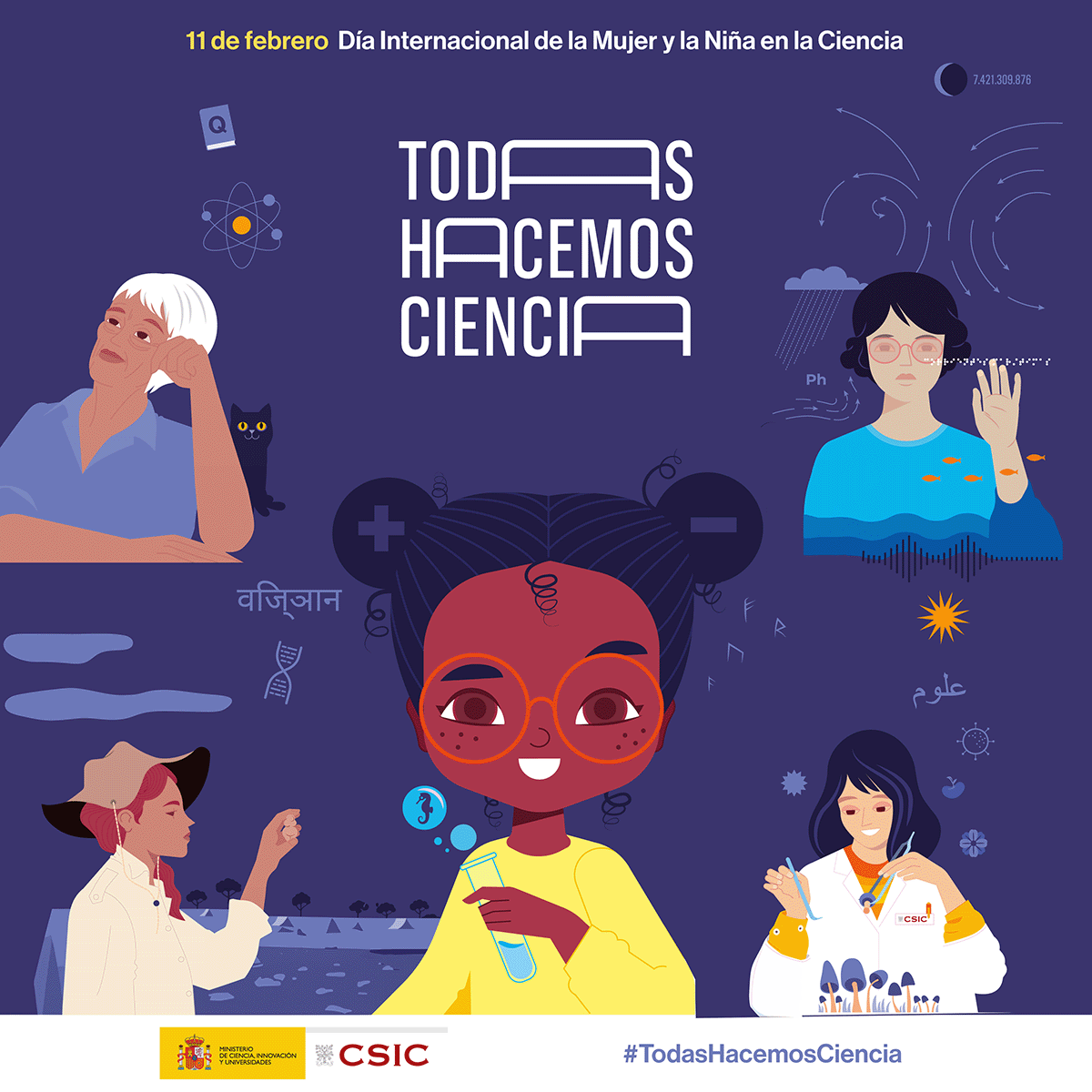
The Institute of Optics joins the celebration of 11F
Full and equal access and participation of women and girls in science and technology Madrid / January 31, 2025In recent decades, the international...

Optoplasmonic tuneable response by femtosecond laser irradiation of glass with deep-implanted gold nanoparticles
Ion implantation of Au2+ at MeV energies has enabled the creation of nanoparticles embedded at greater depth, resulting in a Fabry-Perot cavity...

On November 20th, David Grojo from CNRS will give a lecture entitled “New Dimensions Open to Ultrafast Laser Material Modifications”
Madrid / November 13, 2024On Wednesday, November 20th at 11:30 a.m. we will have a seminar organized by the Laser Processing Group in the conference...