Transparent high conductive Titanium oxynitride nanofilms obtained by nucleation control for sustainable optolectronics

Did you know that it is very difficult to get transparent and electrically conductive materials?
Thin films that are both conductive and transparent are very interesting because they have become essential electrodes for optoelectronic applications. They are used for example in displays for electronic devices and in photovoltaic solar cells.
Indium Tin Oxide (ITO) is the transparent conductor par excellence with 80% transparency and very little electrical resistance.
However, ITO is toxic, fragile and very expensive due to the scarcity of indium in the earth’s crust. Therefore, better and more sustainable alternatives are being sought.
Titanium oxynitrides (TiON) are a very interesting alternative. Titanium is abundant, resistant, non-toxic and its oxynitrides have good electrical and optical properties that can also be adapted to every need by modifying the N / O ratio.
However, achieving the balance between transparency and conductivity to design a suitable and quality electrode is a significant milestone.
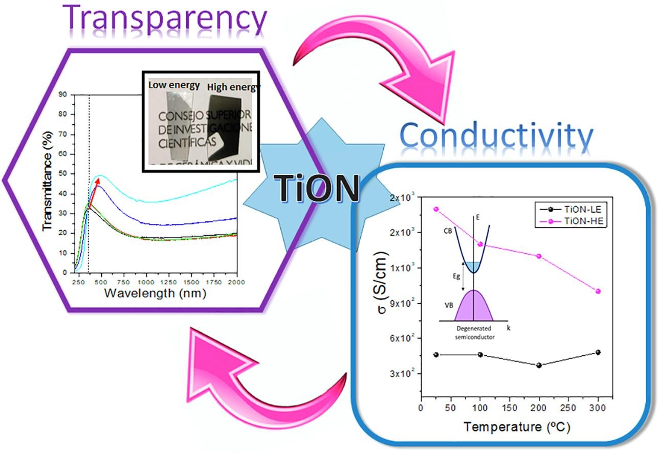
In this work, the scientific team has prepared different high-quality TiON nanofilms (78 nm) by means of PLD (pulsed laser deposition) in vacuum, modifying the transparency and conduction properties by varying the energy of the deposition laser to control the N / O ratio.
A lower energy leads to a TiO2 phase with a lower TiN contribution (16%), while a higher fluence produces a greater amount of TiN (23%).

By manufacturing them in a vacuum, it has been achieved that the films do not have defects and a transparency of up to 50% and a conductivity similar to that of ITO has been achieved.
These results open a new line of research for the development of transparent and sustainable conductive electrodes based on dense and flat TION films, which will be used for the screens of our electronic devices and solar cells.
What is pulsed laser deposition?
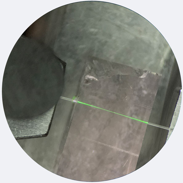
This method of manufacturing thin films of various materials consists of the application of short, high-energy pulses on a material, which we call target and which we place in a vacuum chamber. When the laser hits with high energy, the material vaporizes, forming a plasma that contains the components of the original material in the form of atoms and ions. When this plasma reaches the substrate that we put in front of the target, it is deposited, covering it and forming a thin film. With the energy of the laser and by changing the number of pulses, different thicknesses can be achieved and the properties of the sheet can be varied.
Conductive and transparent materials
Transparent conductive oxides (TCO) have attracted much interest in recent decades due to the increased use of displays for electronic devices and their use in photovoltaic solar cells for renewable energy. They are based on transparent conductive films, which is not an easy goal as transparency is often associated with a low carrier density and therefore a low electrical conductivity typical of glass. Transparent conductive oxides are generally based on doped semiconductors and must have intermediate behavior between metals, which have high carrier density and low mobility, and semiconductors, which have low carrier density and high mobility, in order to combine both properties to achieve high transparency and high conductivity.
Among these materials, indium tin oxide is the material most used today as a transparent conductor because it has a transmittance of 80% in the visible range and an electrical resistivity of 10 −4 Ω · cm, with thicknesses between 15 and 100 nm. However, indium is a very rare element in nature, its extraction is a growing problem, and its toxicity can cause damage to the health of workers. In addition to this, its manufacturing limitations, such as its fragility and lack of flexibility, makes it look for alternatives especially for large displays.
This is a collaborative work between the Optics Institute, the Ceramic and Glass Institute and the Information Technology Department of the Higher Polytechnic School, CEU-San Pablo University


